


2N3906 P-Channel Transistor 40V 0.2A
2,00 EGP
ترانزستور 2N3906 مناسب للصيانة ودوائر التشغيل والتجارب الإلكترونية.
2N3906 Transistor Overview
The 2N3906 Transistor supports switching, driving and amplification tasks in electronic circuits. Technicians choose this transistor when a repair or prototype needs the same package, polarity and rating shown in the product title.
Moreover, this product works well for customers who want a clear component listing before ordering from Electrolik. Therefore, the page focuses on the real product name, the visible model and the category instead of adding unconfirmed technical claims.
2N3906 Transistor Features
- Useful for switching and driver circuits
- Suitable for repair and component replacement work
- Model code helps identify the correct part
- Works well in educational electronics experiments
Specifications
| Product name | 2N3906 P-Channel Transistor 40V 0.2A |
| Model / code | 2N3906 |
| Component type | Transistor |
| Voltage mentioned | 40V |
| Current mentioned | 0.2A |
Applications
Use it in power stages, signal control, small driver circuits or repair boards according to the real circuit design. In addition, compare the datasheet pinout and electrical limits before soldering, because similar packages can still use different pin arrangements.
Usage Notes
In addition, the product title gives the most reliable known details, so the description avoids unsupported specifications. As a result, you can compare the part by model, category and application without relying on guessed values. Also, keep the component away from heat, mechanical stress and reverse wiring during testing. For best results, inspect the board pads, clean the contacts and test the circuit gradually after installation.
For related items, browse the relevant Electrolik category. For general background, you can also read more on Wikipedia.
شرح عربي مختصر
ترانزستور أو موسفت مناسب لأعمال الصيانة والتجارب الإلكترونية ودوائر التشغيل والتحكم. قبل التركيب، راجع ترتيب الأطراف والقيم المطلوبة في الدائرة الأصلية حتى تختار البديل الصحيح بدون تحميل زائد.
ملاحظات الاستخدام
- تأكد من رقم الموديل قبل الشراء.
- راجع الداتا شيت أو الدائرة الأصلية عند الاستبدال.
- اختبر التوصيل تدريجيًا بعد التركيب.
- استخدمه داخل حدود الدائرة المناسبة فقط.
محتويات العبوة
قطعة واحدة من 2N3906 P-Channel Transistor 40V 0.2A حسب الاختيار المتاح في صفحة المنتج.
Related products
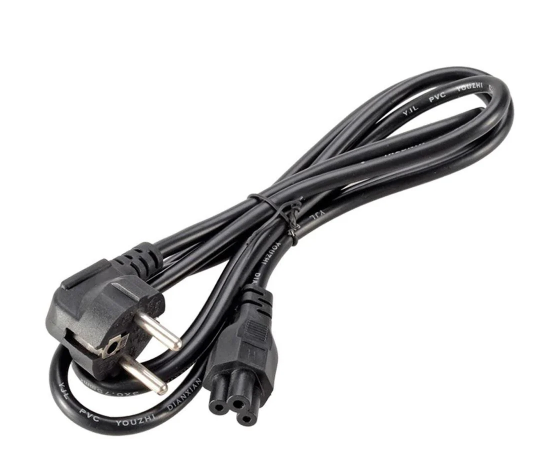
Power Cable for laptop 1.5m
In stock


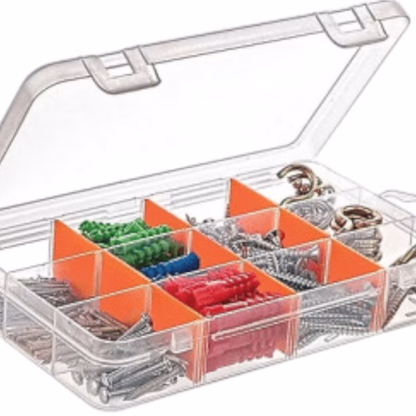
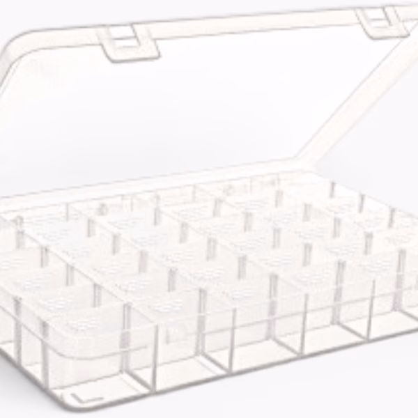
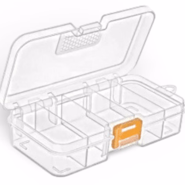
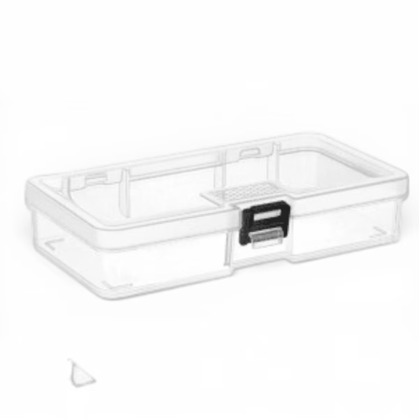
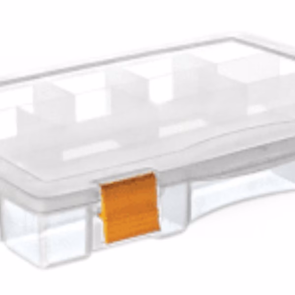
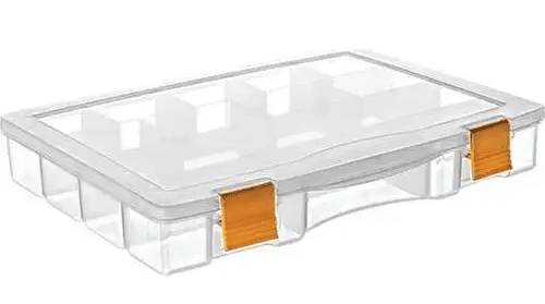
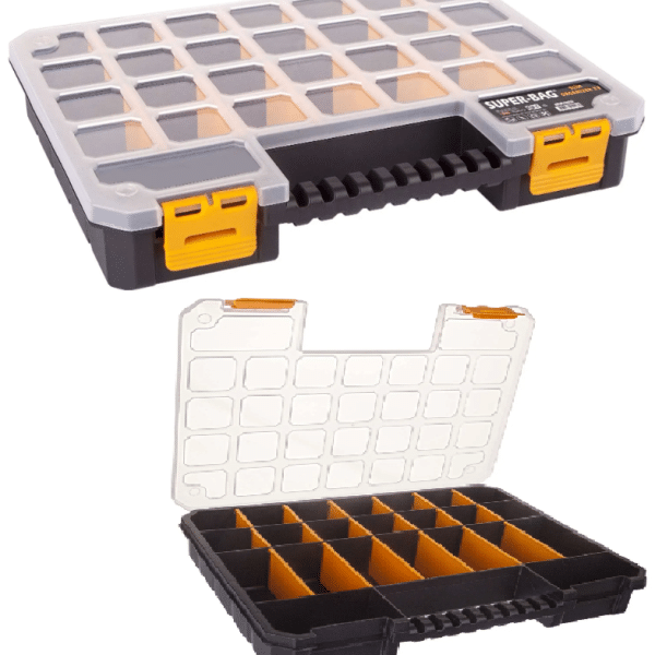
Alpha Double Sided Organizer-10 213x125x50mm ASR-5020
Out of stock

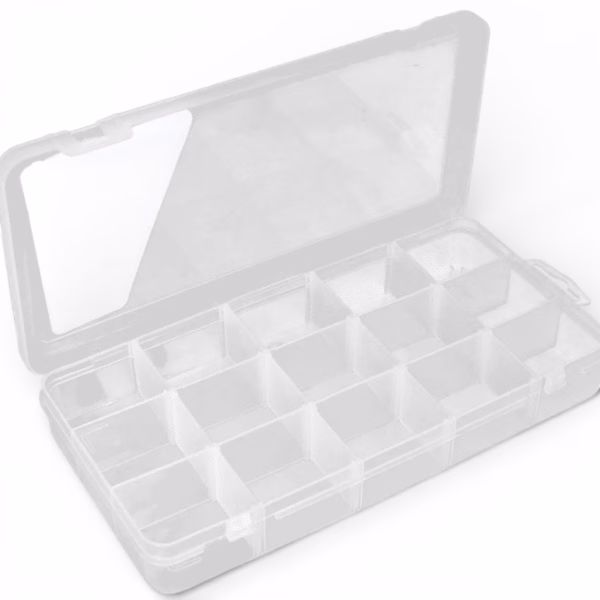
Alpha Double Sided Organizer-8 169x115x50mm ASR-5019
Out of stock

Female DC Power Socket Jack Prewired
In stock
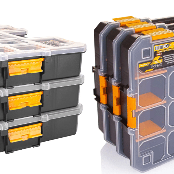
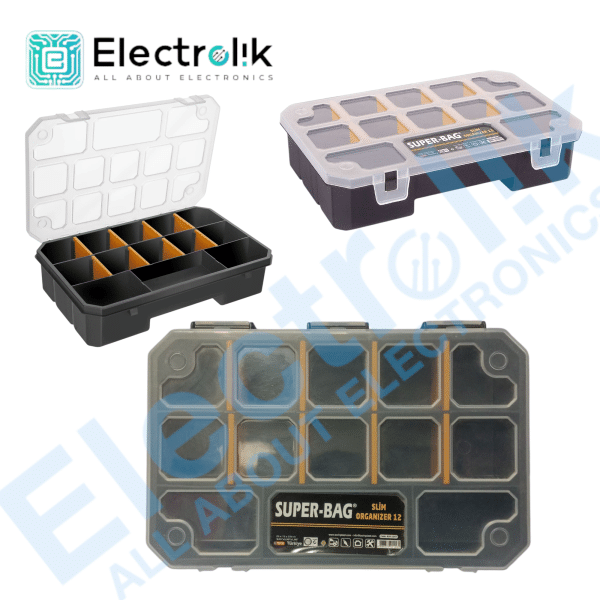
Beta Organizer-12 170x100x30mm ASR-2093
Out of stock
Beta Organizer-15 200x100x30mm ASR-2094
Out of stock

Beta Organizer-25 230x166x42.5mm ASR-5048
Out of stock
Beta Organizer-36 275x195x42.5mm ASR-5049
Out of stock


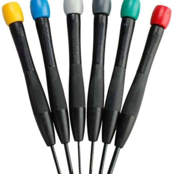


GTK-2114 12in 1 mini screw driver series TOOL KIT Made in Taiwan
Out of stock


JL-1162 31 In 1 Screwdriver Set
In stock


Power Organizer Box-12 9 Inch ASR-2063
Out of stock
Power Organizer Box-13 11 Inch ASR-2064
Out of stock


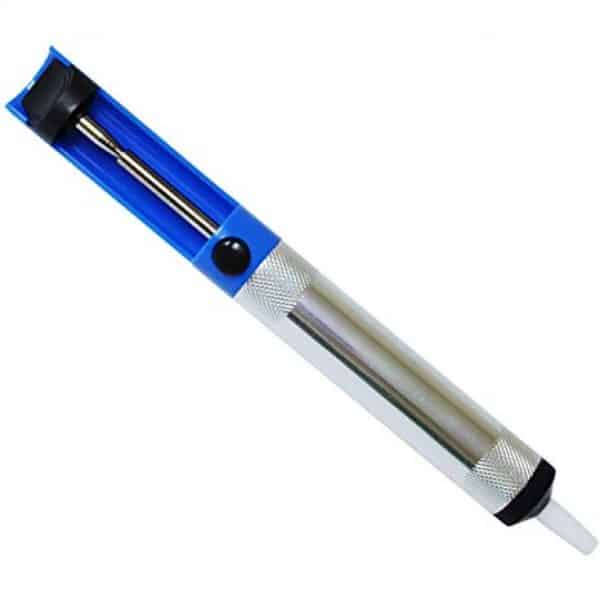
Desoldering Pump ( silver * blue )
In stock


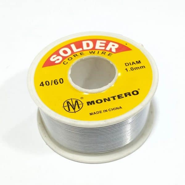
Replacement Toot JAPAN Soldering Irons 60W Tip Normal Size
In stock


Pin Header male (2.54mm) 1X40 Straight
In stock


Reviews
Clear filtersThere are no reviews yet.