


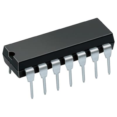
4503 DIP HEX NON-INVERTING BUFFER WITH TRISTATE
12,10 EGP
4503 DIP HEX NON-INVERTING BUFFER WITH TRISTATE
4503 DIP HEX NON-INVERTING BUFFER WITH TRISTATE OUTPUTS: الحل الأمثل لعزل وتوجيه حافلات البيانات
تُعد شريحة 4503 DIP HEX NON-INVERTING BUFFER WITH TRISTATE OUTPUTS (CD4503B) دائرة متكاملة متخصصة من فئة CMOS، مصممة خصيصاً لتطبيقات واجهات حافلات البيانات عالية الأداء. تحتوي هذه الشريحة على ستة مُخففات (Buffers) مستقلة غير عاكسة. يوفر كل مُخفف قدرة كبيرة على إمداد وسحب التيار. الميزة الرئيسية لهذه الشريحة هي هيكل الإخراج ذو الحالات الثلاث (Tri-State). يتيح هذا الهيكل فصل المخرجات إلكترونياً عن خط الحافلة المشترك. يقسم التصميم المنطقي المخففات الستة إلى مجموعتين: يتحكم مدخل تعطيل واحد () في المخففات من الأول إلى الرابع، بينما يتحكم مدخل تعطيل ثانٍ ومستقل () في المخففين الخامس والسادس. يمنح هذا التحكم المُجزأ مرونة فائقة في تصميمات البنية القائمة على الحافلات المعقدة. تضمن شريحة 4503 DIP HEX NON-INVERTING BUFFER WITH TRISTATE OUTPUTS حداً أدنى من تدهور الإشارة. كما تؤمن نقل بيانات نظيفاً ومعزولاً حتى عند وجود أحمال ذات سعة عالية.
مرونة التحكم الموجهة بالحافلات
يوفر نظام التحكم ثنائي المستوى لشريحة 4503 ميزة استراتيجية في تصميم النظام الرقمي.
- وظيفة الإخراج ثلاثي الحالات: عندما يكون مدخل التعطيل المعني ( أو ) في مستوى (منخفض)، يعمل المخفف بشكل طبيعي. يعكس المخرج إشارة الإدخال (غير عاكس). يؤدي تطبيق مستوى (مرتفع) على مدخل التعطيل إلى إجبار المخرجات المقابلة على الدخول في حالة ممانعة عالية (). يفصل هذا الإجراء المخفف كهربائياً عن حافلة البيانات.
- مجموعتا تعطيل مزدوجة: يقسم التصميم المخففات إلى مجموعة من أربعة ومجموعة من اثنين. هذا يسمح بالتحكم الانتقائي في تدفق البيانات. يمكن مثلاً استخدام أربعة خطوط لبيانات أولية، ويتم تخصيص الخطين المتبقيين للتحكم. تعمل الدوائر المنطقية القوية لشريحة 4503 DIP HEX NON-INVERTING BUFFER WITH TRISTATE OUTPUTS على تضخيم جميع الخطوط الستة.
- قدرة قيادة عالية: يتمتع هذا المخفف بقدرة فائقة على التعامل مع التيار. يمكنه قيادة العديد من أحمال CMOS بكفاءة. كما يمكنه قيادة أحمال TTL قياسية عبر نطاق درجة الحرارة بالكامل. هذا يلغي الحاجة إلى مراحل قيادة خارجية في العديد من سيناريوهات الواجهة.
موثوقية CMOS للأنظمة الحساسة
تم تصميم شريحة 4503 DIP HEX NON-INVERTING BUFFER WITH TRISTATE OUTPUTS باستخدام منطق CMOS من الفئة B. هذا يوفر أداءً حاسماً للتشغيل الموثوق به وطويل الأمد.
- جهد تشغيل واسع: تعمل الشريحة بشكل موثوق عبر نطاق واسع من جهد الإمداد، عادةً من إلى . تضمن هذه المرونة سهولة التكامل مع معايير الطاقة المختلفة.
- تبديد منخفض للطاقة: بصفتها جهاز CMOS، يظل استهلاك الطاقة الساكن منخفضاً بشكل ملحوظ. يعد هذا عاملاً بالغ الأهمية في التصميمات الموفرة للطاقة أو التي تعمل بالبطارية.
- خصائص تبديل متماثلة: تتميز المخرجات بأوقات ارتفاع وهبوط متماثلة. كما تقوم الشريحة بموازنة تأخيرات التشغيل والإيقاف. هذا يضمن انتقال إشارة نظيفاً ويمكن التنبؤ به أثناء عمليات نقل البيانات عالية السرعة.
- مناعة ضد الضوضاء والحماية: يوفر الجهاز مناعة عالية ضد الضوضاء. تحتوي الدوائر المتكاملة على حماية مدمجة ضد التفريغ الكهروستاتيكي (). هذا يعزز موثوقية شريحة 4503 في البيئات الكهربائية الصعبة.
تطبيقات رئيسية في الواجهات
إن القدرة المخففة وذات الحالة الثلاثة تجعل هذه الدائرة المتكاملة ضرورية لعدة وظائف رقمية شائعة.
- واجهة حافلة البيانات: إنها المكون المثالي لتوصيل دوائر متكاملة متعددة بحافلة بيانات مشتركة. تضمن أن جهازاً واحداً فقط يقود الحافلة في أي وقت، مما يمنع تضارب الإشارات.
- ترجمة CMOS إلى TTL: تسمح قدرة تيار الخرج العالية للجهاز بربط منطق CMOS الأبطأ والأعلى جهداً بمدخلات TTL القياسية ذات الجهد المنخفض بكفاءة.
- عزل الإشارة: تتيح وظيفة الحالة الثلاثة لمصممي النظام عزل مجموعات من دوائر المنطق مؤقتاً عن بقية النظام. هذا لا يقدر بثمن أثناء اختبار النظام، أو إدارة الطاقة، أو إجراءات التشخيص للأجهزة.
Related products
Reviews
Clear filtersThere are no reviews yet.