

74646 LOGIC GATE
60,50 EGP
74646 LOGIC GATE
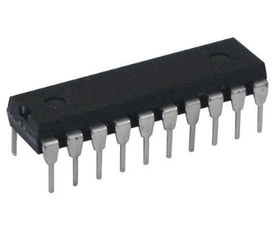
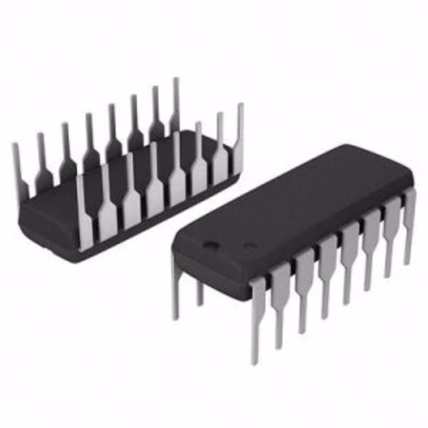
74646 Octal Bus Transceiver and D-Latch with Integrated Parity Generator
The 74646 Octal Bus Transceiver and D-Latch with Integrated Parity Generator offers a high-utility solution for complex digital systems. It merges three critical functions onto a single chip. These functions are an Octal Bus Transceiver, an Octal D-Type Transparent Latch, and a dedicated Parity Generator/Checker. This deep integration significantly reduces board space. It also streamlines data flow and enhances system reliability. Error detection is standardized within the chip.
The transceiver section enables asynchronous, bi-directional data transfer. This happens between two separate 8-bit buses (Bus A and Bus B). Internal D-Latches provide temporary storage for data. This stored data passes through the transceiver. This ensures data integrity during synchronous cycles. This combination is essential in microprocessor-based systems. It enables complex data paths and I/O buffering. The 74646 Octal Bus Transceiver and D-Latch with Integrated Parity Generator is built with advanced Low-Power Schottky (LS) or High-Speed CMOS (HC) technology. This construction ensures fast switching speeds. It also maintains low power consumption. This makes the IC highly suitable for high-throughput applications.
74646 LOGIC GATE
Key Operational Features
The 74646’s triple-function design gives designers powerful control. It also provides vital error-checking capabilities for bus-oriented systems:
- Octal Bus Transceiver (A to B, B to A): This section controls the direction of 8-bit data flow. It manages data transfer between the A bus and the B bus. Dedicated Direction (DIR) and Output Enable () pins manage the data transfer. They also control the tri-state outputs.
- Transparent Octal D-Latch: Internal latches provide intermediate, non-volatile data storage. The latches are transparent when the Latch Enable (LE) pin is High. This means data passes straight through. When LE goes Low, the latches hold the current 8-bit data. This effectively captures a moment in time.
- Integrated Parity Logic: The on-chip Parity Generator/Checker is a unique feature. This circuit automatically calculates even or odd parity for the 8-bit data stream on Bus A. It outputs a Parity Error signal () if the received parity does not match the expected setting.
- Asynchronous Clear (): A clear pin allows immediate, asynchronous resetting of the internal latches. This provides necessary initialization capability. It does not rely on the clock cycle.
74646 LOGIC GATE
Technical Advantages and System Benefits
The comprehensive integration offered by the 74646 delivers tangible performance and reliability benefits. These benefits surpass systems using three separate ICs:
- Minimized Component Count: The 74646 combines three functions. It reduces the need for external drivers, latches, and error detection logic. This saves substantial PCB real estate.
- Enhanced Data Integrity: The automatic, high-speed parity checking improves the reliability of data. This is crucial for data transferred between boards or over noisy communication lines.
- Power and Speed Balance: The device is manufactured using modern logic processes (e.g., HC). This guarantees fast propagation delays. This speed is necessary for high-speed microprocessors. It achieves this while drawing minimal static current.
- Simplified Design Flow: The logical pinout and unified control structure simplify the design process. This helps in establishing complex, controlled data transfer protocols in embedded systems.
Application Environments
The robust functionality of the 74646 Octal Bus Transceiver and D-Latch with Integrated Parity Generator makes it essential in several critical system areas:
- High-Reliability Computing: It is used in medical and aerospace systems. In these systems, data errors must be detected immediately.
- Microprocessor I/O Ports: It functions as an I/O port buffer and transceiver. This is ideal for peripheral control and memory interfaces.
- Bus Isolation and Buffering: It provides galvanic isolation and current boosting. This is useful for system buses extending across multiple modules or racks.
- Data Acquisition Systems: It temporarily holds sampled data. This data is then used for subsequent synchronous processing by a microcontroller or DSP.
This device is an optimized, multi-function solution. It is designed to increase the efficiency and integrity of modern synchronous and asynchronous data buses.
Related products


S8036 SOP8 for Mini Receiver IC Signal or Power Compatible with Sunplus Receiver
In stock


Reviews
Clear filtersThere are no reviews yet.